- 您现在的位置:买卖IC网 > Sheet目录343 > MIC4223YM (Micrel Inc)IC MOSFET DVR DUAL-INV 4A 8-SOIC
Micrel, Inc.
MIC4223/MIC4224/MIC4225
Application Information
Power Dissipation Considerations
Power dissipation in the driver can be separated into two
areas:
Output driver stage dissipation
Quiescent current dissipation used to supply the
internal logic and control functions.
Output Driver Stage Power Dissipation
Power dissipation in the driver’s output stage is mainly
caused by charging and discharging the gate to source
and gate to drain capacitance of the external MOSFET.
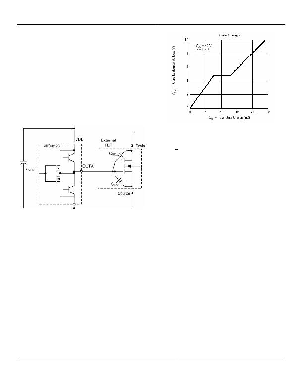
Figure 3 shows a simplified circuit of the MIC4223 driving
an external MOSFET.
Figure 4. MOSFET Gate Charge vs. V GS
The energy dissipated during turn-on is calculated as:
E = 1 2 × C iss × V GS
2
where C iss is the MOSFET' s total gate capacitanc e
but :
Q = C × V
so
E = 1/2 × Q G × V GS
An equivalent amount of energy is dissipated in the
Figure 3. Functional MOSFET/Driver Diagram
Dissipation Caused by Switching the External
MOSFET
Energy from capacitor C VDD is used to charge up the input
capacitance of the MOSFET (C GD and C GS ). The energy
delivered to the MOSFET is dissipated in the upper driver
MOSFET and Bipolar impedances. The effective
capacitance of C GD and C GS is difficult to calculate since
they vary non-linearly with I D , V GS , and V DS . Fortunately,
most power MOSFET specifications include a typical
graph of total gate charge vs. V GS . Figure 4 shows a
typical MOSFET gate charge curve. The graph illustrates
that for a gate voltage of 10V, the MOSFET requires about
23.5nC of charge.
driver’s sink circuit when the MOSFET turns off. The total
energy and power dissipated by the drive components is:
E DRIVER = Q G × V GS
and
P DRIVER = Q G × V GS × f S
Where:
E DRIVER is the energy dissipated per switching cycle
P DRIVER is the power dissipated by switching the
MOSFET on and off
Q G is the total Gate charge at V GS
V GS is the MOSFETs Gate to Source voltage
f S is the switching frequency of the Gate drive
circuit
June 2009
10
M9999-061109-A
(408) 944-0800
发布紧急采购,3分钟左右您将得到回复。
相关PDF资料
MIC4417YM4 TR
IC DRIVER MOSF LOW SIDE SOT143-4
MIC4420ZT
IC DRIVER MOSFET 6A LS TO-220-5
MIC4422AYN
IC DRIVER MOSFET 9A LS 8-DIP
MIC4422ZT
IC DRIVER MOSFET 9A LS TO-220-5
MIC4424YWM
IC DRIVER MOSFET 3A DUAL 16-SOIC
MIC4427YM
IC DRIVER MOSFET DUAL 1.5A 8SOIC
MIC4451ZT
IC DRIVER MOSFET 12A HS TO220-5
MIC4467YWM
IC DRIVER MOSF QUAD 1.2A 16-SOIC
相关代理商/技术参数
MIC4223YM TR
功能描述:功率驱动器IC Dual 4A High Speed MOSFET Drivers with Enable
RoHS:否 制造商:Micrel 产品:MOSFET Gate Drivers 类型:Low Cost High or Low Side MOSFET Driver 上升时间: 下降时间: 电源电压-最大:30 V 电源电压-最小:2.75 V 电源电流: 最大功率耗散: 最大工作温度:+ 85 C 安装风格:SMD/SMT 封装 / 箱体:SOIC-8 封装:Tube
MIC4223YMME
功能描述:功率驱动器IC Dual 4A High Speed MOSFET Drivers with Enable
RoHS:否 制造商:Micrel 产品:MOSFET Gate Drivers 类型:Low Cost High or Low Side MOSFET Driver 上升时间: 下降时间: 电源电压-最大:30 V 电源电压-最小:2.75 V 电源电流: 最大功率耗散: 最大工作温度:+ 85 C 安装风格:SMD/SMT 封装 / 箱体:SOIC-8 封装:Tube
MIC4223YMME TR
功能描述:功率驱动器IC Dual 4A High Speed MOSFET Drivers with Enable
RoHS:否 制造商:Micrel 产品:MOSFET Gate Drivers 类型:Low Cost High or Low Side MOSFET Driver 上升时间: 下降时间: 电源电压-最大:30 V 电源电压-最小:2.75 V 电源电流: 最大功率耗散: 最大工作温度:+ 85 C 安装风格:SMD/SMT 封装 / 箱体:SOIC-8 封装:Tube
MIC4224
制造商:MICREL 制造商全称:Micrel Semiconductor 功能描述:Dual 4A, 4.5V to 18V, 15ns Switch Time, Low-Side MOSFET Drivers with Enable
MIC4224YM
功能描述:功率驱动器IC Dual 4A High Speed MOSFET Drivers with Enable
RoHS:否 制造商:Micrel 产品:MOSFET Gate Drivers 类型:Low Cost High or Low Side MOSFET Driver 上升时间: 下降时间: 电源电压-最大:30 V 电源电压-最小:2.75 V 电源电流: 最大功率耗散: 最大工作温度:+ 85 C 安装风格:SMD/SMT 封装 / 箱体:SOIC-8 封装:Tube
MIC4224YM TR
功能描述:功率驱动器IC Dual 4A High Speed MOSFET Drivers with Enable
RoHS:否 制造商:Micrel 产品:MOSFET Gate Drivers 类型:Low Cost High or Low Side MOSFET Driver 上升时间: 下降时间: 电源电压-最大:30 V 电源电压-最小:2.75 V 电源电流: 最大功率耗散: 最大工作温度:+ 85 C 安装风格:SMD/SMT 封装 / 箱体:SOIC-8 封装:Tube
MIC4224YMME
功能描述:功率驱动器IC Dual 4A High Speed MOSFET Drivers with Enable
RoHS:否 制造商:Micrel 产品:MOSFET Gate Drivers 类型:Low Cost High or Low Side MOSFET Driver 上升时间: 下降时间: 电源电压-最大:30 V 电源电压-最小:2.75 V 电源电流: 最大功率耗散: 最大工作温度:+ 85 C 安装风格:SMD/SMT 封装 / 箱体:SOIC-8 封装:Tube
MIC4224YMME TR
功能描述:功率驱动器IC Dual 4A High Speed MOSFET Drivers with Enable
RoHS:否 制造商:Micrel 产品:MOSFET Gate Drivers 类型:Low Cost High or Low Side MOSFET Driver 上升时间: 下降时间: 电源电压-最大:30 V 电源电压-最小:2.75 V 电源电流: 最大功率耗散: 最大工作温度:+ 85 C 安装风格:SMD/SMT 封装 / 箱体:SOIC-8 封装:Tube
